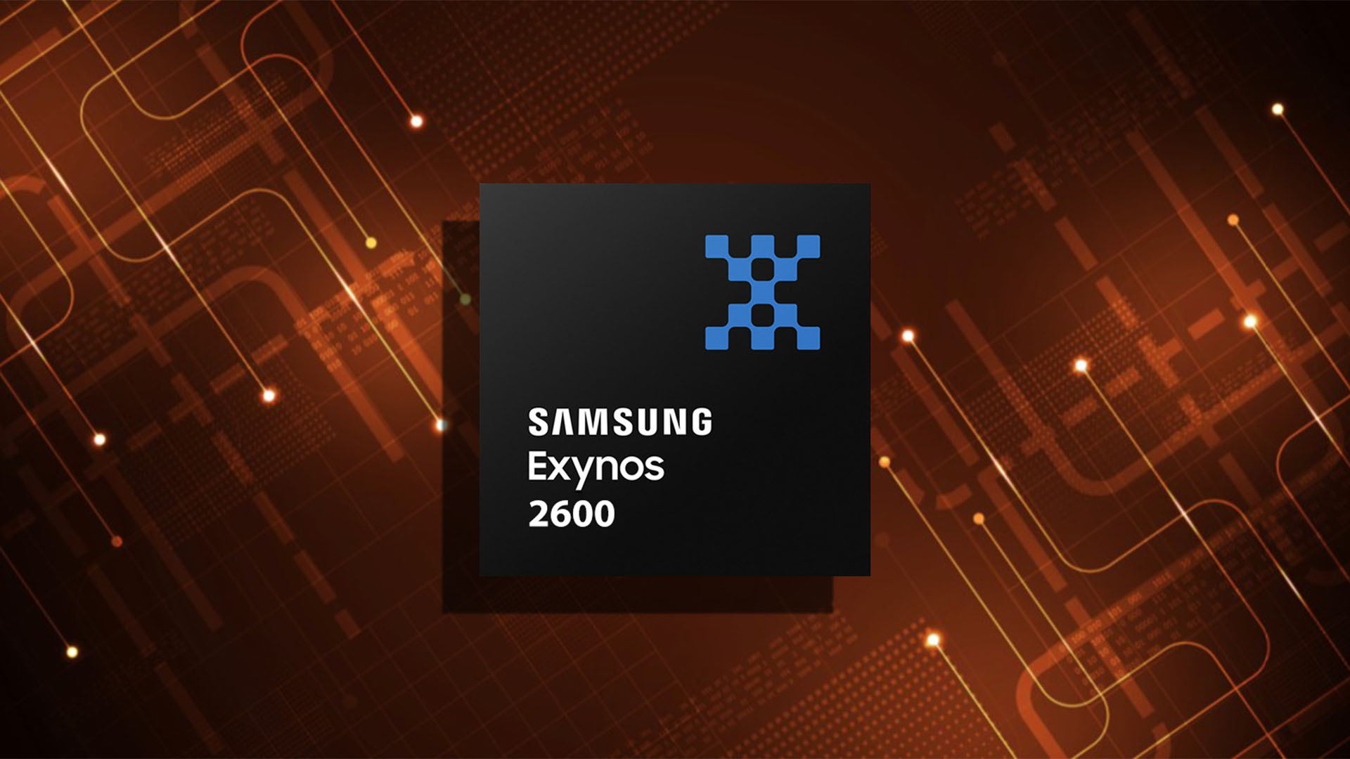
The Blueprint is Out: Samsung's Next-Gen Silicon Detailed
Just weeks after Samsung officially teased its return to flagship smartphone chipsets, the most comprehensive specifications for the Exynos 2600 have surfaced online. A coordinated leak from renowned tipsters, including Ice Universe (PhoneArt), has laid bare the CPU architecture, clock speeds, and graphics details of what will be the world's first 2nm smartphone processor.
The leaks, corroborated by reports from SamMobile, Android Authority, and GSMArena, paint a picture of a chip designed for strong multi-core performance and advanced graphics, built on Samsung's cutting-edge 2nm Gate-All-Around (GAA) fabrication process. This silicon is widely expected to power the standard Galaxy S26 and S26+ models in several regions, marking a significant comeback for Samsung's in-house Exynos division.
Anatomy of a Flagship Chip: CPU, GPU & Process
Exynos 2600 CPU Cluster Configuration
Up to 3.9GHz
3.25GHz
2.75GHz
The leaked 1+3+6 "deca-core" (10-core) configuration.
CPU Architecture
The headline is the 10-core CPU arranged in a tri-cluster setup:
- Prime Core: 1x high-power core clocked at 3.9GHz (some reports note 3.8GHz).
- Performance Cores: 3x cores running at 3.25GHz.
- Efficiency Cores: 6x cores humming at 2.75GHz.
This configuration is based on Arm's new Lumex platform, which also brings improvements to AI performance. The design philosophy appears focused on delivering robust multi-threaded performance rather than chasing the absolute highest single-core clock speeds.
AMD RDNA Graphics ('JUNO')
The graphics portion continues Samsung's collaboration with AMD. The GPU, codenamed 'JUNO' and likely to be marketed as the Xclipse 960, is a key highlight.
It's based on AMD's RDNA architecture and supports modern graphics APIs including OpenGL ES 3.2, OpenCL 3.0, and Vulkan 1.3. Early reports suggested this GPU could be highly competitive, though real-world performance in the final Galaxy S26 hardware remains to be seen.
2nm GAA Fabrication
The foundational advantage of the Exynos 2600 is its manufacturing process.
- Node: Samsung Foundry's 2nm Gate-All-Around (GAA) process.
- Goal: Major efficiency gains and reduced power consumption compared to previous Exynos chips.
- Challenge: Reports suggest the 2nm process may limit maximum stable clock speeds, which is why the prime core may cap at ~3.8-3.9GHz instead of going higher.
Samsung is reportedly employing new Heat Path Block technology to manage thermals, addressing a long-standing criticism of Exynos chips.
Performance Implications & Galaxy S26 Strategy
Early Benchmark Context: A Geekbench listing for the Exynos 2600 showed scores of approximately 3,455 (single-core) and 11,621 (multi-core). For reference, a leak for a Snapdragon 8 Elite Gen 5 device showed ~3,078 and 9,162 points, respectively, though these numbers are not from final hardware.
The 10-core design strongly suggests Samsung is targeting class-leading multi-core performance and sustained workloads, potentially excelling in productivity, advanced photo/video editing, and gaming. The single-core speed, while high, may trail the peak clocks of competitors like the Snapdragon 8 Elite Gen 5.
The Galaxy S26 Divide: Consistent leaks point to a split strategy for the upcoming flagship series:
- Galaxy S26 & S26+: Will use the Exynos 2600 in many regions (e.g., South Korea, Europe), but are expected to ship with the Snapdragon 8 Elite Gen 5 in the US, Canada, and China.
- Galaxy S26 Ultra: Is expected to use the Snapdragon chip globally, without an Exynos variant.
If Samsung has successfully solved the efficiency and thermal issues of past Exynos chips, the Exynos 2600 could finally deliver consistent flagship performance across regions, a long-requested feature from Samsung fans.